𝘈 𝘭𝘰𝘰𝘬 𝘢𝘵 𝘵𝘩𝘦 𝘦𝘲𝘶𝘪𝘱𝘮𝘦𝘯𝘵 & 𝘱𝘳𝘰𝘤𝘦𝘴𝘴𝘦𝘴 𝘴𝘵𝘢𝘯𝘥𝘪𝘯𝘨 𝘣𝘦𝘵𝘸𝘦𝘦𝘯 𝘺𝘰𝘶𝘳 𝘣𝘰𝘢𝘳𝘥 𝘥𝘦𝘴𝘪𝘨𝘯 & 𝘢 𝘥𝘦𝘧𝘦𝘤𝘵𝘪𝘷𝘦 𝘴𝘩𝘪𝘱𝘮𝘦𝘯𝘵.
Every PCB order carries the same risk: a board that looks perfect on the outside but fails once it’s soldered, powered on or exposed to the field.
Warpage from lamination, hidden corrosion under a gold finish, a plating void buried inside a via — none of these show up on a visual inspection line. They show up in your product, months later, as a return or a field failure.
This is why we built our quality control program around three specific failure modes that account for the majority of multilayer PCB defects: dimensional expansion/shrinkage after lamination, nickel corrosion under ENIG finishes and hidden internal structural defects.
Here’s exactly how we catch them — and why it matters to whoever is signing off on your next PO.
𝟭. 𝗘𝘅𝗽𝗮𝗻𝘀𝗶𝗼𝗻 & 𝗦𝗵𝗿𝗶𝗻𝗸𝗮𝗴𝗲 𝗖𝗼𝗻𝘁𝗿𝗼𝗹: 𝗞𝗲𝗲𝗽𝗶𝗻𝗴 𝗘𝘃𝗲𝗿𝘆 𝗟𝗮𝘆𝗲𝗿 𝗶𝗻 𝗥𝗲𝗴𝗶𝘀𝘁𝗿𝗮𝘁𝗶𝗼𝗻
Multilayer boards move during lamination. Heat and pressure cause the laminate to expand and then shrink slightly as it cools. If that shift isn’t measured and compensated for, your inner layers drift out of alignment with the outer layers (misregistration).
In a dense multilayer design, even a small drift can mean a via that no longer lands on its target pad.
How we control it:
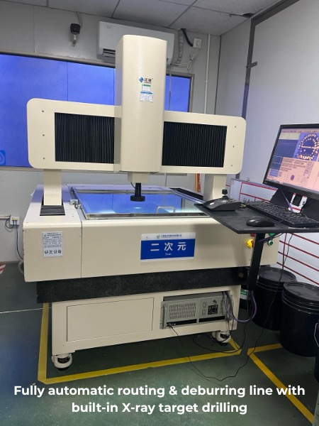
• 𝘍𝘶𝘭𝘭𝘺 𝘢𝘶𝘵𝘰𝘮𝘢𝘵𝘪𝘤 𝘳𝘰𝘶𝘵𝘪𝘯𝘨 & 𝘥𝘦𝘣𝘶𝘳𝘳𝘪𝘯𝘨 𝘭𝘪𝘯𝘦 𝘸𝘪𝘵𝘩 𝘣𝘶𝘪𝘭𝘵-𝘪𝘯 𝘟-𝘳𝘢𝘺 𝘵𝘢𝘳𝘨𝘦𝘵 𝘥𝘳𝘪𝘭𝘭𝘪𝘯𝘨 𝘮𝘢𝘤𝘩𝘪𝘯𝘦. After lamination, this system uses X-ray imaging to locate fiducial targets buried in the internal layers, the same targets it can still find even after the panel has physically shifted.
From there, it calculates the exact scaling and distortion factors for that specific panel and feeds real-time compensation into the router, so the final cut lands on true design dimensions, not on the panel’s shifted geometry.
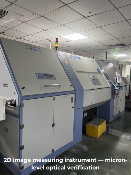
• 2𝘋 𝘪𝘮𝘢𝘨𝘦 𝘮𝘦𝘢𝘴𝘶𝘳𝘪𝘯𝘨 𝘪𝘯𝘴𝘵𝘳𝘶𝘮𝘦𝘯𝘵. Our independent check on that process. Using non-contact optical measurement, it verifies hole position, outline profile and pad-to-edge spacing at micron-level accuracy on the finished board, effectively re-measuring the router’s work before it leaves the building.
The workflow, in three steps:
→ measure expansion/shrinkage data during drilling
→ route and cut with real-time compensation
→ independently verify result with offline optical sampling
Three separate checkpoints.
Why it matters: layer-to-layer registration is invisible on a finished board until you’re deep into assembly, or worse, in the field. Catching drift before shipment means you’re not the one who finds it.
In the next post, we’ll talk about how we solve the “black pad” problem before it reaches customers…