
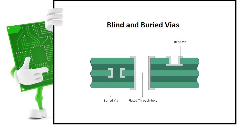
Blind and buried vias are needed when the PCB circuit artwork or design is of very tight or heavy packaging density that would not allow a via or vias to pass entirely through all the layers of the circuit board without interfering with another electrical feature.
Blind vias are used to connect an outer layer to the next adjacent inner layer. Buried vias will generally connect any two adjacent layers. Some PCBs may contain combinations of either process to meet a design need.
While the technology is widely available, the budget for these more expensive circuit boards may not be.
An additional drilling, or multiple drilling processes, along with associated plating baths will be required. The costlier process of laser drilling may be involved, along with the time-consuming process of controlled depth drilling (one panel height at a time.)
The process to manufacture a blind and/or buried via printed circuit board is known as sequential lamination. It is essentially the manufacture of a simple 2-layer circuit board that is bonded to the required additional outer layers, which is then sent through the normal processes of drill and plating to complete the circuit card.
Basically, for each set of blind and/or buried vias, the cost for an additional plated through layer is required, not to mention the cost consideration from the fallout or scrap from each of those individual builds.
You can imagine the cost factor for the above graphic, which shows a 6-layer PCB with blind and buried vias. Layers 3 and 4 are processed as a double-sided board and then it is laminated between layers 1 and 2, and layers 5 and 6.
Layers 1 and 2 contain a blind via that was created through either the use of laser drilling or controlled depth drilling, along with an additional plating process to achieve connection between the layers 1 and 2.
Because of the numerous steps in the manufacture of this type of circuit board, the quoting process for this technology will take longer—but shouldn’t be more than an extra day—as compared to standard technology.
Need to know more about PCB manufacturing or buying? Reach out to me at greg@directpcb.com.
Click here to get a free copy of my book, PCB Basics for Buyers.