𝘈 𝘭𝘰𝘰𝘬 𝘢𝘵 𝘵𝘩𝘦 𝘦𝘲𝘶𝘪𝘱𝘮𝘦𝘯𝘵 & 𝘱𝘳𝘰𝘤𝘦𝘴𝘴𝘦𝘴 𝘴𝘵𝘢𝘯𝘥𝘪𝘯𝘨 𝘣𝘦𝘵𝘸𝘦𝘦𝘯 𝘺𝘰𝘶𝘳 𝘣𝘰𝘢𝘳𝘥 𝘥𝘦𝘴𝘪𝘨𝘯 & 𝘢 𝘥𝘦𝘧𝘦𝘤𝘵𝘪𝘷𝘦 𝘴𝘩𝘪𝘱𝘮𝘦𝘯𝘵.
𝐂𝐫𝐨𝐬𝐬-𝐒𝐞𝐜𝐭𝐢𝐨𝐧 𝐂𝐨𝐧𝐭𝐫𝐨𝐥: 𝐒𝐞𝐞𝐢𝐧𝐠 𝐖𝐡𝐚𝐭’𝐬 𝐀𝐜𝐭𝐮𝐚𝐥𝐥𝐲 𝐈𝐧𝐬𝐢𝐝𝐞 𝐭𝐡𝐞 𝐁𝐨𝐚𝐫𝐝
A PCB’s outer layers can look flawless while copper-thickness variation, interlayer delamination and through-hole plating voids remain entirely hidden. The only way to know for certain is to look inside the board. That’s what cross-section analysis does.
How we control it:
• 𝘈𝘶𝘵𝘰𝘮𝘢𝘵𝘪𝘤 𝘚𝘢𝘮𝘱𝘭𝘪𝘯𝘨 𝘔𝘢𝘤𝘩𝘪𝘯𝘦: A low-speed diamond saw precisely cuts a sample from the required location. Slow, controlled cutting avoids heat damage that could distort or mask the structure we’re examining.
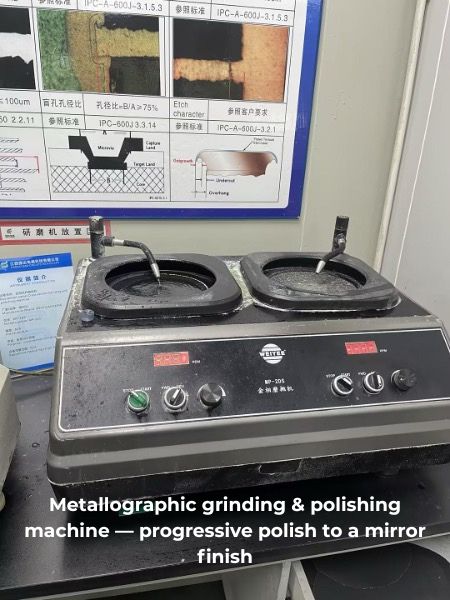
• 𝘔𝘦𝘵𝘢𝘭𝘭𝘰𝘨𝘳𝘢𝘱𝘩𝘪𝘤 𝘎𝘳𝘪𝘯𝘥𝘪𝘯𝘨 & 𝘗𝘰𝘭𝘪𝘴𝘩𝘪𝘯𝘨 𝘔𝘢𝘤𝘩𝘪𝘯𝘦: The sample is ground through progressively finer abrasive grits and polished to a scratch-free mirror finish, revealing true copper thickness and plating detail rather than cutting artifacts.
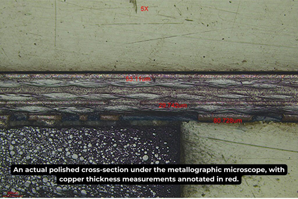
• 𝘔𝘦𝘵𝘢𝘭𝘭𝘰𝘨𝘳𝘢𝘱𝘩𝘪𝘤 𝘔𝘪𝘤𝘳𝘰𝘴𝘤𝘰𝘱𝘦: High-magnification 2D imaging of the polished cross-section lets us measure via and through-hole copper thickness, detect delamination or voids and evaluate plating uniformity. This is our workhorse for routine batch verification.
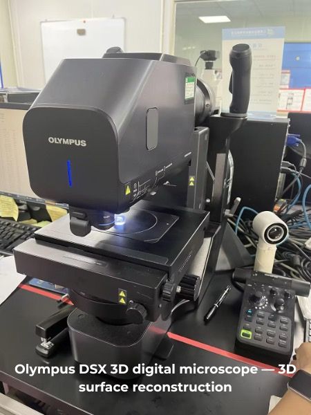
• 𝘋𝘚𝘟 3𝘋 𝘋𝘪𝘨𝘪𝘵𝘢𝘭 𝘔𝘪𝘤𝘳𝘰𝘴𝘤𝘰𝘱𝘦: For cases needing more than a flat image, this system reconstructs a three-dimensional surface model from multiple focal planes, directly measuring pad flatness, corrosion pit depth and delamination gap width rather than estimating them from a 2D cross-section.
It’s the tool we reach for on high-standard shipment verification and detailed nickel corrosion analysis.
The sample workflow:
→ grind and polish to a mirror finish
→ observe under metallographic or 3D microscopy
Every step preserves the true internal structure. We measure what’s actually there, not a cutting or polishing artifact.
Why it matters: no amount of surface inspection will catch internal defects. Cross-section verification confirms what’s inside every batch instead of just what’s visible on top.
𝐓𝐡𝐞 𝐁𝐨𝐭𝐭𝐨𝐦 𝐋𝐢𝐧𝐞
None of this equipment exists merely to check a box on a quality certificate. Dimensional drift, nickel corrosion and internal structural defects are the three failure modes most likely to turn into your problem after the board leaves our dock. Each requires a purpose-built method to catch before shipment.
This process runs behind every panel we ship. We’re glad to walk through inspection reports, cross-section samples or SEM/EDS data for any batch.
𝙍𝙚𝙖𝙘𝙝 𝙤𝙪𝙩 𝙩𝙤 𝙨𝙖𝙡𝙚𝙨@𝙙𝙞𝙧𝙚𝙘𝙩𝙥𝙘𝙗.𝙘𝙤𝙢 for more information!